- 您现在的位置:买卖IC网 > Sheet目录3872 > PIC16CR77T-I/ML (Microchip Technology)IC PIC MCU 8KX14 44QFN
PIC18F2220/2320/4220/4320
DS39599G-page 146
2007 Microchip Technology Inc.
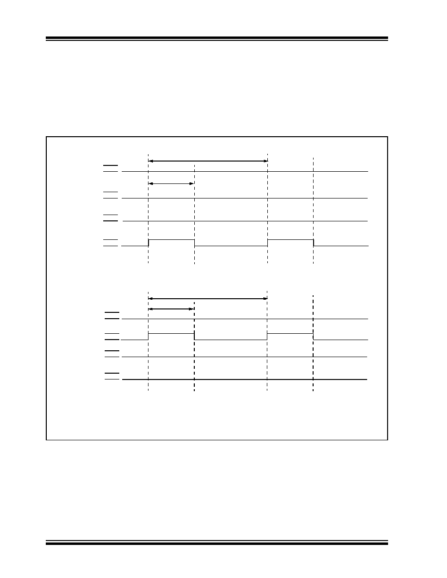
16.4.3
FULL-BRIDGE MODE
In Full-Bridge Output mode, four pins are used as out-
puts; however, only two outputs are active at a time. In
the Forward mode, pin RC2/CCP1/P1A is continuously
active and pin RD7/PSP7/P1D is modulated. In the
Reverse mode, RD6/PSP6/P1C pin is continuously
active and RD5/PSP5/P1B pin is modulated. These are
illustrated in Figure 16-6.
P1A, P1B, P1C and P1D outputs are multiplexed with
the PORTC<2> and PORTD<5:7> data latches. The
TRISC<2> and TRISD<5:7> bits must be cleared to
make the P1A, P1B, P1C and P1D pins output.
FIGURE 16-6:
FULL-BRIDGE PWM OUTPUT
Period
Duty Cycle
P1A(2)
P1B(2)
P1C(2)
P1D(2)
FORWARD MODE
(1)
Period
Duty Cycle
P1A(2)
P1C(2)
P1D(2)
P1B(2)
REVERSE MODE
(1)
Note 1: At this time, the TMR2 register is equal to the PR2 register.
Note 2: Output signal is shown as active-high.
发布紧急采购,3分钟左右您将得到回复。
相关PDF资料
PIC24F16KA102-I/SO
IC PIC MCU FLASH 16K 28-SOIC
PIC18F45K20-I/PT
IC PIC MCU FLASH 16KX16 44TQFP
PIC16CR77-I/PT
IC PIC MCU 8KX14 44TQFP
PIC16F884-I/ML
IC PIC MCU FLASH 4KX14 44QFN
PIC16CR77-I/P
IC PIC MCU 8KX14 40DIP
PIC18F45K20-I/MV
MCU 32KB FLASH 1536B RAM 40-UQFN
PIC16CR76T-I/SS
IC PIC MCU 8KX14 28SSOP
PIC18F13K50-I/P
IC PIC MCU FLASH 4KX16 20-PDIP
相关代理商/技术参数
PIC16CR77T-I/PT
功能描述:IC PIC MCU 8KX14 44TQFP RoHS:是 类别:集成电路 (IC) >> 嵌入式 - 微控制器, 系列:PIC® 16C 产品培训模块:Asynchronous Stimulus
8-bit PIC® Microcontroller Portfolio 标准包装:42 系列:PIC® 16C 核心处理器:PIC 芯体尺寸:8-位 速度:20MHz 连通性:- 外围设备:欠压检测/复位,POR,PWM,WDT 输入/输出数:13 程序存储器容量:3.5KB(2K x 14) 程序存储器类型:OTP EEPROM 大小:- RAM 容量:128 x 8 电压 - 电源 (Vcc/Vdd):4 V ~ 5.5 V 数据转换器:A/D 4x8b 振荡器型:外部 工作温度:-40°C ~ 85°C 封装/外壳:18-SOIC(0.295",7.50mm 宽) 包装:管件 配用:XLT18SO-1-ND - SOCKET TRANSITION 18SOIC 300MILISPICR1-ND - ADAPTER IN-CIRCUIT PROGRAMMING309-1011-ND - ADAPTER 18-SOIC TO 18-DIP309-1010-ND - ADAPTER 18-SOIC TO 18-DIPAC164010-ND - MODULE SKT PROMATEII DIP/SOIC
PIC16CR83T-04/SO023
制造商:Microchip Technology Inc 功能描述:
PIC16F
制造商:Microchip Technology Inc 功能描述:Microchip PIC16F677-I/P Microcontroller
PIC16F1454-E/ML
制造商:Microchip Technology Inc 功能描述:7 KB FLASH, 512 BYTES RAM, 48 MHZ INT. OSC, 12 I/0, ENHANCED - Rail/Tube 制造商:Microchip Technology Inc 功能描述:IC MCU 8BIT 7KB FLASH 16QFN
PIC16F1454-E/P
制造商:Microchip Technology Inc 功能描述:7 KB FLASH, 512 BYTES RAM, 48 MHZ INT. OSC, 12 I/0, ENHANCED - Rail/Tube 制造商:Microchip Technology Inc 功能描述:IC MCU 8BIT 7KB FLASH 14PDIP
PIC16F1454-E/SL
制造商:Microchip Technology Inc 功能描述:7 KB FLASH, 512 BYTES RAM, 48 MHZ INT. OSC, 12 I/0, ENHANCED - Rail/Tube 制造商:Microchip Technology Inc 功能描述:IC MCU 8BIT 7KB FLASH 14SOIC
PIC16F1454-E/ST
制造商:Microchip Technology Inc 功能描述:7 KB FLASH, 512 BYTES RAM, 48 MHZ INT. OSC, 12 I/0, ENHANCED - Rail/Tube 制造商:Microchip Technology Inc 功能描述:IC MCU 8BIT 7KB FLASH 14TSSOP 制造商:Microchip Technology Inc 功能描述:8-bit Microcontrollers - MCU 7KB Flsh 512b RAM 48MHz Int Osc 12 I/0
PIC16F1454-I/ML
功能描述:8位微控制器 -MCU 7 KB Flash 512 bytes RAM 48 MHz Int Osc
RoHS:否 制造商:Silicon Labs 核心:8051 处理器系列:C8051F39x 数据总线宽度:8 bit 最大时钟频率:50 MHz 程序存储器大小:16 KB 数据 RAM 大小:1 KB 片上 ADC:Yes 工作电源电压:1.8 V to 3.6 V 工作温度范围:- 40 C to + 105 C 封装 / 箱体:QFN-20 安装风格:SMD/SMT